


Technical Approach for Diamond Growth on Silicon: MPCVD
In today's era of rapid advancement in chip technology, the integration density of chips continues to rise, with transistor counts proliferating like mushrooms after rain across silicon wafers no larger than a fingernail. However, as chip manufacturing processes advance from 14nm towards 3nm and beyond, the physical limitations of traditional silicon materials are becoming increasingly apparent. Transistors resemble ‘highly dense, three-dimensional nanoscale structures’ compressed into minuscule spaces, where silicon-based materials are proving increasingly inadequate in terms of thermal efficiency and structural stability. This has become a critical bottleneck constraining further improvements in chip performance.
Diamond: The Saviour of Chip Performance
Confronted with this predicament, scientists turned their attention to diamond. Beyond its striking appearance, diamond possesses exceptionally high thermal conductivity and stable physicochemical properties, making it an ideal material for resolving chip heat dissipation and stability issues. By ‘teaming up’ with chips, diamond holds the promise of overcoming the performance limitations of silicon-based materials, paving new pathways for chip technology advancement.
Technical Challenges in Diamond Growth on Silicon Substrates
To achieve this powerful synergy between diamond and silicon-based chips, a core issue must be resolved: how to ensure diamond compatibility with current mainstream silicon semiconductor manufacturing processes? This necessitates breakthroughs in the most critical technical aspect—growing high-quality diamond films on silicon substrates.
Technical Approach for Diamond Growth on Silicon: MPCVD
The technical pathway for diamond growth on silicon parallels that of silicon carbide epitaxial growth, both fundamentally relying on CVD (Chemical Vapour Deposition) technology. Currently, the mainstream technique for preparing diamond films on silicon wafers is MPCVD (Microwave Plasma Chemical Vapor Deposition). Its core principle involves using microwave energy to excite reaction gases into a plasma state, which then provides the energy for chemical reactions, ultimately depositing high-quality diamond films onto the silicon substrate surface.
The four key steps of the MPCVD (Microwave Plasma Chemical Vapor Deposition) process can be summarised as follows:
Injection of Reaction Gases: Initial preparatory steps involve placing the silicon wafer substrate into the reaction chamber, evacuating the chamber, and heating the substrate to 700–1000°C. Subsequently, gases containing carbon atoms are introduced into the reaction chamber to provide feedstock for subsequent chemical reactions.
Microwave-excited plasma generation: The microwave generator is activated, producing high-frequency microwaves transmitted into the reaction chamber. Upon absorption by the methane-hydrogen mixture, the microwave energy breaks molecular bonds within the gas molecules. This ionisation generates numerous charged particles, including electrons, hydrogen ions, and carbon radicals, ultimately forming the plasma.
Plasma chemical reactions: High-energy particles within the plasma (such as electrons and reactive free radicals) collide violently with methane molecules, triggering a series of complex chemical reactions. This process resembles a ‘screening mechanism,’ where only carbon atoms meeting the structural requirements of diamond crystals are retained to participate in subsequent thin-film growth.
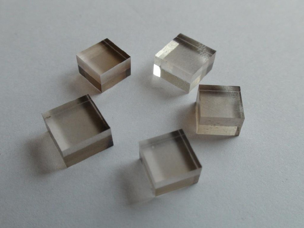
Diamond Film Growth: The selected active carbon atoms are transported to the surface of the silicon substrate wafer. They then slowly ‘migrate’ to suitable positions, stacking layer by layer according to the fixed structural rules of diamond crystals. This process ultimately forms a continuous, dense diamond film that is tightly bonded to the silicon substrate.
Control of Process Parameters and Equipment Requirements
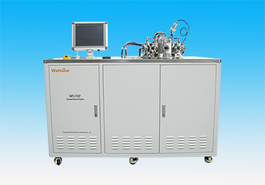
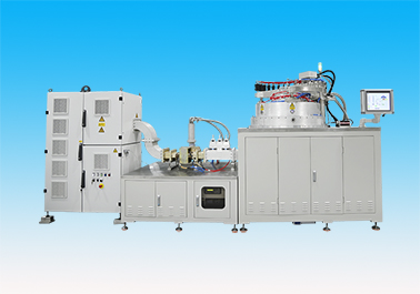
By adjusting key parameters such as microwave power, reaction gas composition ratios, and substrate temperature, the crystalline quality, thickness, and surface morphology of diamond films can be effectively controlled. To accomplish this series of precise chemical reactions, advanced equipment capable of providing a pure, controllable reaction environment is indispensable—namely, high-power MPCVD systems.
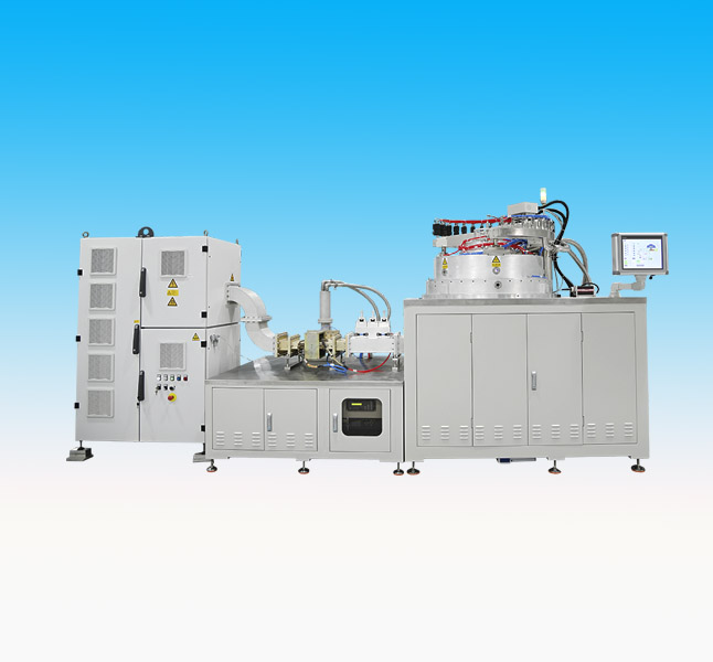
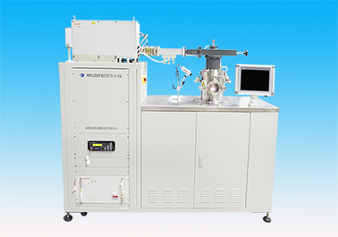
75KW MPCVD Equipment
Diamond, as a material possessing unique properties, holds extensive application prospects within the semiconductor industry. With continuous technological advancements and breakthroughs, the integration of diamond with silicon-based chips will become increasingly seamless, presenting new opportunities and challenges for the semiconductor sector. HUERAY, as an MPCVD manufacturer, believes that in the near future, diamond will emerge as a pivotal material in chip technology, propelling the advancement of human technological progress.
- > The three key advantages ··· 2026-04-14
- > What is large-size MPCVD ··· 2026-03-11
- > MPCVD Equipment: Rising i··· 2026-02-28
- > Diamond Thin Film Deposit··· 2026-01-23
- > CVD Diamond Films Market:··· 2025-12-24
- > Analysing MPCVD Diamond: ··· 2025-12-19
- > 4-inch diamond ultrathin ··· 2025-12-17
- > Technical Approach for Di··· 2025-11-21
Recommended Products