


CVD Diamond Films Market: MPCVD Fuels High-End Applications
Overview of CVD Polycrystalline Diamond Films
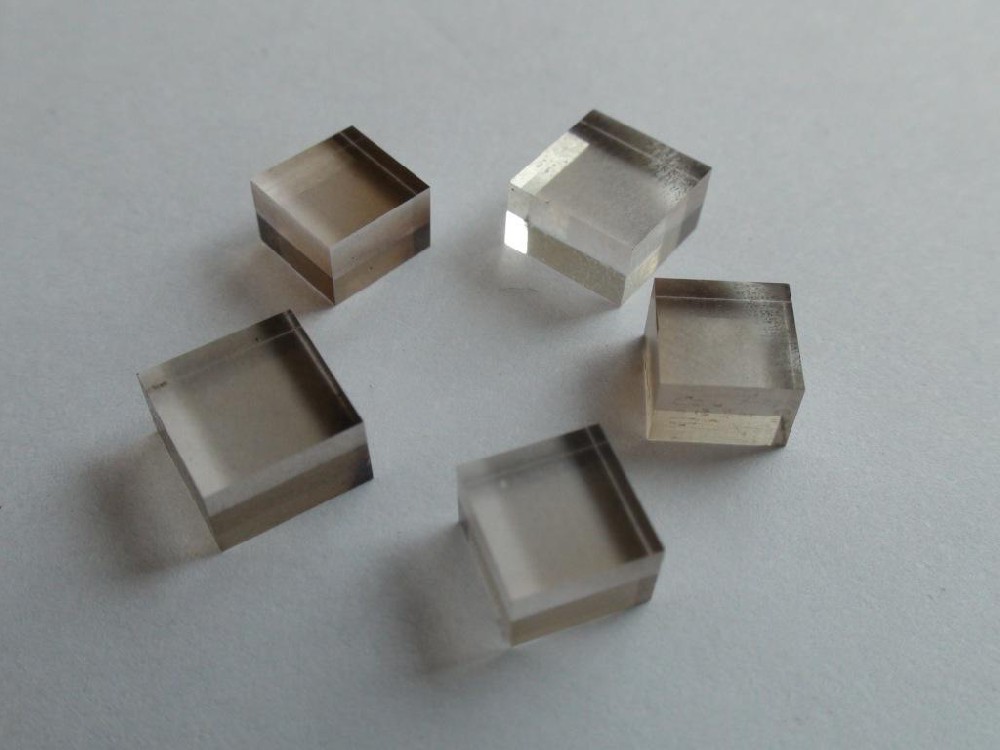
CVD polycrystalline diamond film is an artificial diamond material produced using chemical vapor deposition (CVD) technology. During fabrication, carbon-containing gases decompose in a vacuum chamber, depositing carbon atoms onto a substrate to form a diamond film. Unlike single-crystal diamond, CVD polycrystalline diamond consists of multiple diamond grains with varying orientations and sizes, giving it a polycrystalline structure. This material offers advantages such as lower cost, suitability for large-area and complex-shape coverage, as well as high hardness, wear resistance, and thermal conductivity. It is widely used in cutting tools, wear-resistant coatings, optical components, electronic devices, and heat sinks. Its excellent performance and versatility enable broad adoption across numerous industries that demand high durability and reliability.
Core CVD Diamond Preparation Technologies
The main mainstream preparation techniques currently include the following three methods:
Hot‑filament Chemical Vapor Deposition (HFCVD): Uses a high‑temperature filament (approximately 2000 °C) to decompose hydrocarbons and hydrogen gas. It is characterized by simple equipment, low cost, and suitability for large‑area deposition, and is extensively employed for tool coatings, although the coating quality is generally lower compared to other methods.
Direct Current Plasma‑Enhanced Chemical Vapor Deposition (DC‑PECVD): Uses a direct‑current electric field to excite plasma, enabling low‑temperature (even near‑ambient) deposition. It offers strong film‑substrate adhesion and is suitable for non‑catalytic substrates, showing potential in fields such as photodetectors.
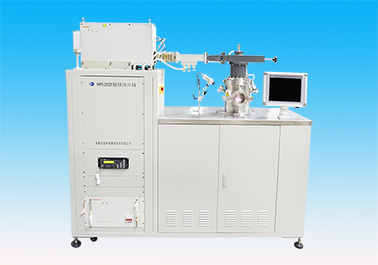
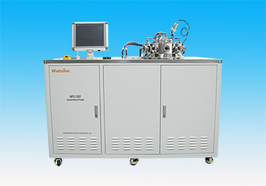
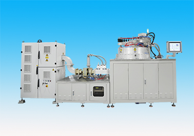
Microwave Plasma Chemical Vapor Deposition (MPCVD): Uses microwave energy to excite plasma, avoiding electrode contamination and enabling the production of high‑quality diamond films.
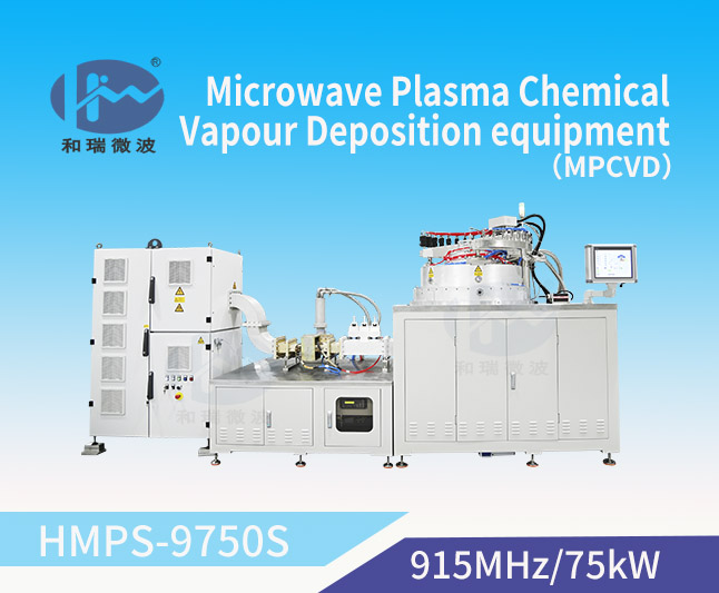
Core Advantages of MPCVD: As the leading technique for producing high‑quality diamond films, its core strengths lie in the purity of the plasma and the absence of electrode contamination. This results in lower defect densities, superior crystalline quality, and higher purity. These characteristics make MPCVD indispensable for cutting‑edge applications that demand exceptional material properties, such as optical‑grade windows, quantum‑information substrates, and high‑power device thermal management. Its fast deposition rates, low energy consumption, clean operation, and outstanding overall material performance establish its technological dominance in high‑end applications.
Global Market Status and Forecast
According to research statistics from DIResearch, the global CVD polycrystalline diamond film market has maintained steady growth. The market size reached ¥2.688 billion (RMB) in 2025 and is projected to reach ¥4.634 billion by 2032, representing a compound annual growth rate (CAGR) of 8.08% from 2025 to 2032. Regionally, the Asia‑Pacific region holds the largest share at approximately 43.61%, followed by Europe and North America at 26.17% and 25.35%, respectively.
Market Segmentation and Application Analysis
CVD polycrystalline diamond films deliver significant value across diverse sectors, with high‑end applications relying primarily on high‑quality materials produced via techniques such as MPCVD:
Quantum Technology: Nitrogen‑doped diamond (NDD) films within electronic‑grade CVD diamond contain NV centers, enabling quantum‑state manipulation and readout at room temperature. These are applicable in quantum sensing and quantum computing, with their long spin‑coherence time enhancing detection sensitivity. The production of such high‑performance films depends heavily on techniques like MPCVD.
Optical Applications: Optical‑grade CVD diamond exhibits broad spectral transparency and strong radiation resistance, making it suitable for high‑end laser systems and optical windows in extreme environments—for example, as light‑transmitting and heat‑dissipating components in tokamak devices. High‑quality optical‑grade diamond is primarily achieved through MPCVD processes.
Energy Sector: High‑purity diamond films are used in nuclear radiation detectors; heat‑sink‑grade films enable efficient thermal dissipation; and boron‑doped diamond (BDD) electrodes, owing to their wide electrochemical window and low overpotential, play a key role in green‑energy technologies such as electrolytic hydrogen production.
Disclaimer: Portions of the textual content are sourced from publicly available online information. Copyright remains with the original authors. Should any infringement occur, please contact the editor for removal.
- > The three key advantages ··· 2026-04-14
- > What is large-size MPCVD ··· 2026-03-11
- > MPCVD Equipment: Rising i··· 2026-02-28
- > Diamond Thin Film Deposit··· 2026-01-23
- > CVD Diamond Films Market:··· 2025-12-24
- > Analysing MPCVD Diamond: ··· 2025-12-19
- > 4-inch diamond ultrathin ··· 2025-12-17
- > Technical Approach for Di··· 2025-11-21
Recommended Products