


Technical Advantages of CVD Diamond and Its Prospects in Semiconductor Applications
Chemical vapour deposition (CVD) diamond has become a key material in the semiconductor field due to its high purity, excellent electrical properties, and scalability in production. Through this paper, MPCVD manufacturer Hueray Microwave systematically analyses the physical properties of CVD diamond, mainstream preparation techniques, and its application potential in the semiconductor industry. It focuses on exploring the technical advantages of microwave plasma chemical vapour deposition (MPCVD) and outlines its path towards driving the next generation of semiconductor technology revolution.
I. Physical and Chemical Properties of CVD Diamond
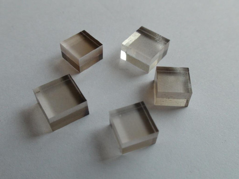
CVD diamond exhibits near-identical composition, structure, and physical properties to natural diamond. Its core advantages lie in purity and electrical performance:
Purity Advantage: Through gas deposition processes, CVD diamond contains negligible metallic impurities (e.g., iron, nickel), achieving significantly higher purity than natural diamond. This satisfies the semiconductor industry's stringent material purity requirements.
Electrical Properties: Exhibiting an exceptionally high breakdown electric field (>10 MV/cm), saturated carrier mobility (>2000 cm²/V·s), and low dielectric constant (ε=5.7), it demonstrates irreplaceable advantages in high-power devices and high-frequency electronic components.
II. CVD Diamond Preparation Technology Systems
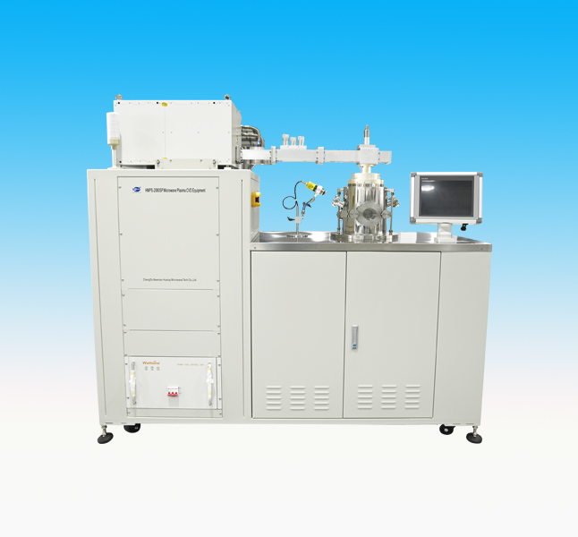
Mainstream CVD diamond deposition techniques in China include:
Hot-wire chemical vapour deposition (HFCVD): Low cost but slow growth rate, prone to hot-wire contamination.
Direct current plasma chemical vapour deposition (DC-PACVD): High energy utilisation but poor plasma stability.
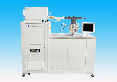
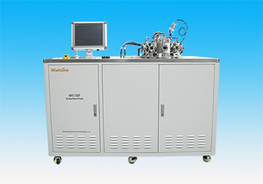
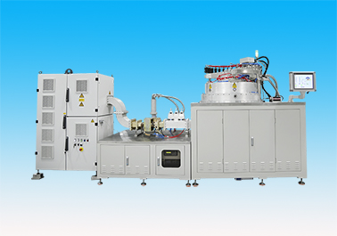
Microwave Plasma Chemical Vapour Deposition (Hueray MPCVD): Utilises microwave-excited plasma to achieve contamination-free, high-purity diamond growth, establishing itself as the current mainstream technology.
Direct Current Arc Plasma Jet Chemical Vapour Deposition (DC Arc Plasma Jet CVD): Suitable for large-area rapid deposition, though characterised by high equipment complexity.
III. Technical Advantages of the MPCVD Method
The MPCVD method stands as the preferred technology for producing high-quality diamonds due to the following characteristics:
Contaminant-free growth environment: Utilises a metal chamber and microwave energy to prevent catalyst incorporation, significantly enhancing crystal quality.
Large-scale diamond production: Overcomes substrate size limitations of conventional equipment, enabling growth of oversized diamonds to provide foundational materials for semiconductor applications.
Process flexibility: Supports diamond film deposition on curved (irregular) surfaces and enables in-situ intermediate layer processing to meet diverse requirements.
Economic Efficiency: Simple operation and low energy consumption result in significantly reduced long-term operating costs compared to other CVD technologies.
IV. Application Prospects of CVD Diamond in the Semiconductor Sector
Large-Scale Diamond Production: As semiconductor industries demand increasingly larger diamond dimensions, MPCVD is advancing single-crystal sizes towards the millimetre scale through optimised process parameters (e.g., pressure, temperature, gas ratios).
Technological Revolution Potential: As CVD equipment costs decrease and processes mature, synthetic diamond holds promise to replace traditional silicon-based materials, enabling breakthroughs in high-temperature, high-frequency, and high-power devices.
Industrial Collaborative Innovation: The deep integration of CVD diamond with semiconductor technology will catalyse next-generation electronic devices, such as diamond-based RF filters and high-power laser packaging.
CVD diamond, leveraging its purity, performance, and fabrication advantages, has become a critical material in the semiconductor field. As the most advanced technological pathway, the MPCVD method is spearheading a new generation of semiconductor technological revolution by driving innovations in the production of large-size single-crystal and polycrystalline diamond and process development. Looking ahead, through industrial collaboration and technological iteration, the application boundaries of CVD diamond will expand further, offering disruptive solutions for the semiconductor industry.
- > The three key advantages ··· 2026-04-14
- > What is large-size MPCVD ··· 2026-03-11
- > MPCVD Equipment: Rising i··· 2026-02-28
- > Diamond Thin Film Deposit··· 2026-01-23
- > CVD Diamond Films Market:··· 2025-12-24
- > Analysing MPCVD Diamond: ··· 2025-12-19
- > 4-inch diamond ultrathin ··· 2025-12-17
- > Technical Approach for Di··· 2025-11-21
Recommended Products