


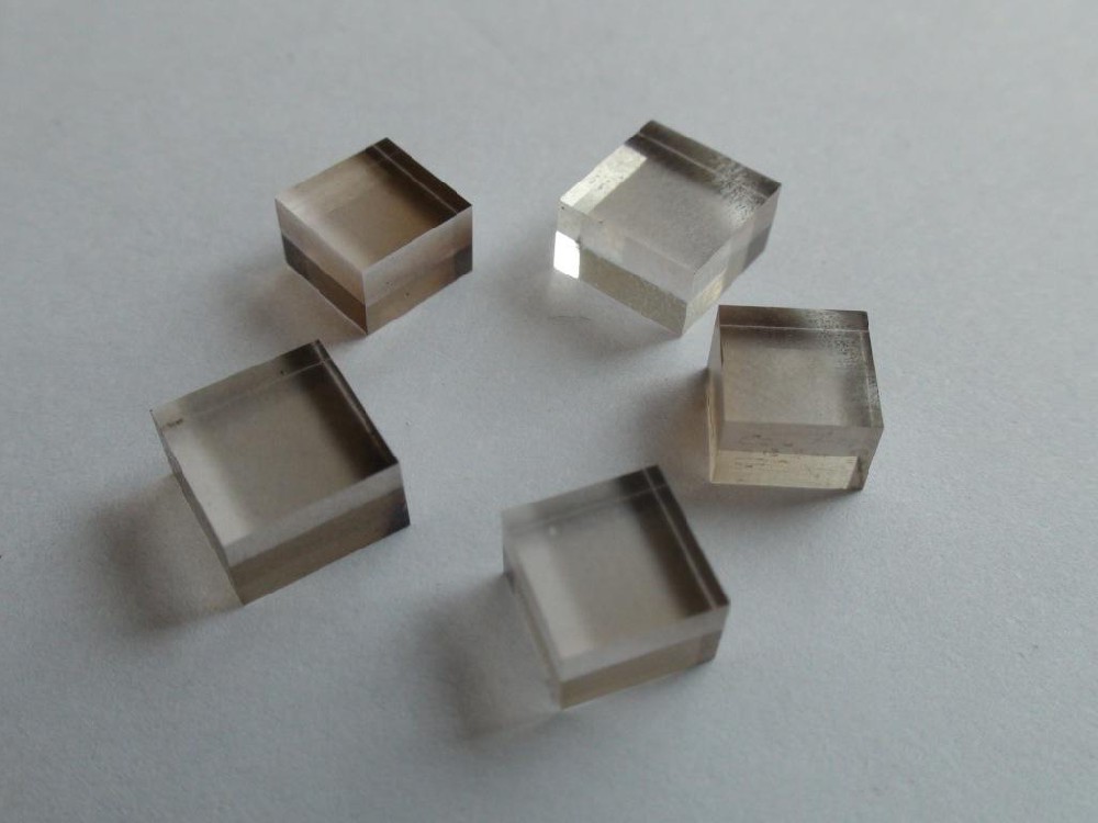


4-inch diamond ultrathin films achieve damage-free self-peeling, enhancing thermal management for se
With electronic devices rapidly advancing towards higher power and greater integration, chip thermal management has become a core bottleneck constraining performance and reliability. Diamond, owing to its exceptionally high thermal conductivity and excellent insulating properties, is regarded as the ideal material for next-generation chip cooling. It plays an irreplaceable role particularly in advanced thermal management solutions such as direct bonding and three-dimensional packaging. Traditional diamond film fabrication typically employs silicon substrates, with silicon removed via chemical etching to yield ‘self-supporting’ diamond films. However, this process suffers from drawbacks including lengthy duration, high cost, and environmental pollution.
Recently, a research team from the Ningbo Institute of Materials Technology and Engineering, Chinese Academy of Sciences, has made significant progress in diamond ultrathin film fabrication technology. The team has successfully developed a ‘self-peeling’ technique for 4‑inch ultra‑low‑warpage diamond ultrathin films. By precisely controlling the diamond nucleation and growth stages and introducing process innovations, the team achieved complete, damage‑free separation of the diamond film from its silicon substrate using only gravity after synthesis. This requires only simple grooving treatment and no external force. The method not only reduces the separation time from several hours—as required in chemical etching—to mere minutes, thereby significantly boosting production efficiency, but also avoids the environmental impact associated with etching processes. It thus pioneers a new pathway for the green, low‑cost manufacturing of high‑quality diamond ultrathin films.
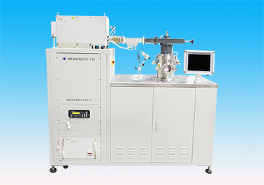
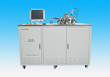
Notably, the successful implementation of this technology relies on advanced deposition equipment. The research team employed a 915MHz MPCVD (Microwave Plasma Chemical Vapour Deposition) apparatus, successfully scaling diamond deposition to 12-inch wafers and achieving simultaneous growth of five 4-inch diamond films per run with low stress and minimal warpage. The high-power, highly uniform plasma environment provided by this equipment offers a critical process foundation for large-area, high-quality, low-stress diamond growth, thereby ensuring the feasibility and stability of subsequent ‘self-peeling’ processes.

Hueray 915MHz MPCVD Equipment
This technological breakthrough, combined with the large-scale deposition capability of the 915MHz MPCVD equipment, signifies the formal transition of ‘self-supporting’ diamond ultrathin film fabrication from laboratory research to industrial-scale batch production. In the future, this technology is expected to find extensive application in high-power chip thermal management for sectors such as 5G communications, high-performance computing, and new energy vehicles. It will drive the continuous advancement of semiconductor devices towards higher power density, greater reliability, and enhanced environmental sustainability.
- > The three key advantages ··· 2026-04-14
- > What is large-size MPCVD ··· 2026-03-11
- > MPCVD Equipment: Rising i··· 2026-02-28
- > Diamond Thin Film Deposit··· 2026-01-23
- > CVD Diamond Films Market:··· 2025-12-24
- > Analysing MPCVD Diamond: ··· 2025-12-19
- > 4-inch diamond ultrathin ··· 2025-12-17
- > Technical Approach for Di··· 2025-11-21
Recommended Products